|
Nitride Thermal Oxide Pyrex Fused Silica Quartz Germanium Zinc Gallium Nitride Gallium Arsenide Sapphire Glass Indium Phosphide Graphene |
|||||||||||||||||||||||||||||||||||||
Solar Wafers |
|||||||||||||||||||||||||||||||||||||
|
Call 800-216-8349 or fax 888-832-0340 or Email Us |
Super-Thin Silicon |
||||||||||||||||||||||||||||||||||||
|
|||||||||||||||||||||||||||||||||||||
|
|
|||||||||||||||||||||||||||||||||||||
|
A Universitywafer.com web site |
|||||||||||||||||||||||||||||||||||||
 |
|||||||||||||||||||||||||||||||||||||
|
SOI Wafers |
|||||||||||||||||||||||||||||||||||||
|
Sapphire |
|||||||||||||||||||||||||||||||||||||
|
|
|||||||||||||||||||||||||||||||||||||
|
Soda Lime * D263 * Wafer Dicing * Indium Tin Oxide * Float Zone * Super-Thin & Flat Wafer Silicon 25um, 50um, 75um, 100um For MEMS |
|
Order Online Here https://order.universitywafer.com |
|
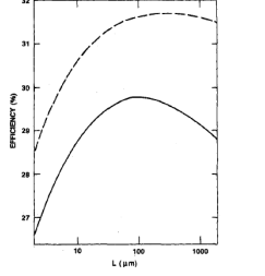
Summary of Solar Cell Production, and Limiting Efficiency of Silicon Solar Cell Limiting Efficiency It has been well established that the limiting efficiency of single crystals falls at about 29% [Swanson] this limit was established in the seminal work by Tiedje. In figure 1 we can see this limiting efficiency as a function of solar cell thickness. In this diagram, the peak efficiency is shown to be 29% with a thickness of just under 100µm
Typical production solar cells achieve about 20% efficiency, while the best laboratory efforts have achieved about 25% [Swanson]. Green provides an excellent summary of the current progress of high-efficiency single-crystal silicon solar cells, and reconfirms the 29% limit established by Tiedje. Production Process The process of manufacturing solar cells from single crystal p-type silicon wafers is detailed below. This is the generalized method used based on a number of sources. It should be noted that different companies have different patented, and trade secret processes for each of these steps, but the steps remain the same. Texturing: N doping (usually Phosphorous): Edge diffusion cleaning: Anti-reflective coating References 1.) Tiedje et al; Limiting Efficiency of Silicon Solar Cells: http://optoelectronics.eecs.berkeley.edu/ey1984ieeeed315.pdf 2.) M.A Green; Progress and outlook for high-efficiency crystalline silicon solar cells http://144.206.159.178/FT/957/22841/412931.pdf 3.) Swanson, R.M; Approaching the 29% limit efficiency of silicon solar cells http://ieeexplore.ieee.org/xpl/login.jsp?tp=&arnumber=1488274&url=http%3A%2F %2Fieeexplore.ieee.org%2Fxpls%2Fabs_all.jsp%3Farnumber%3D1488274 4.) Solar Cell production process http://www.photonics.com/Article.aspx?AID=40098 5.) Solar cell production video: http://www.youtube.com/watch?v=TRATu_wEgAY 6.) Solar Cell production video: http://www.youtube.com/watch?v=fZ1SC-vUe_I
|
|
|
