|
142706
I am interested in your new bonding service. Can you bond glass-to-glass at low temperature with a hermetic seal? Can you bond wafers that have already been fabricated?
-
Yes, we can bond glass-to-glass
at low temperature with a hermetic seal. Bu this client need to know that the plant uses a propitiatory spin-on polymer to achieve this, not anodic bonding.
Wafers that have already been fabricated can be bonded
too as long as surfaces are clean and polished.
Thanks for asking, let us know if further questions.
-
Do you know what temperature they will see?
-
Curing temperature from 70 to 200C
depending on polymer/solvent concentration we are going to use for your application. You can suggest us your temperature preference, lower or higher. Thanks,
-
The curing temperature is fantastic, anywhere in
that temperature range is great. Since this is a R&D project, some things may change over time, so I have a couple of other questions. Right now, we are looking a bonding just the edges of two 125mm wafers
together. Later, we may want to bond a grid type pattern over the wafers.
· How wide would the lines have to be to ensure a hermetic
seal?
· Can you bond the wafers in argon?
· If we have metal on top of the glass (copper, nickel, Ti, or TiW) would
you be able to provide a hermetic seal?
· How thick is the material, for initial tests it would be helpful to have a film greater than 15 microns, later we could design
around pretty much any thickness.
This should be the last of the questions. I appreciate your help.
-
Can the client tell more specifications of the bonding need? We need info on wafer
material, size, thickness, and surface finish, and requirement on bonding profile. For now, it looks like he just needs sealing two flat wafers only along wafer edges, but this is not a bonding technology to do the
job.
-
The final material will be either glass or quartz, optically polished. We are currently using 125mm diameter, Borofloat glass, 0.7mm thick, optically polished.
These are
patterned wafers with materials <15 microns in height above the surface of the wafer. If the bonding material is greater than 15 microns, then we will use a flat Borofloat wafer as the cap. If the bonding
material is <15 microns, then we can etch a cavity into the glass cap to provide room for the devices.
I need to know what is meant be "requirement on bonding profile" or you referring to the thermal
profile? If so, we would prefer to stay <300C due to the mismatch in CTE between materials on the devices and the glass.
-
As mentioned before, the plant uses a spin-on polymer as bonding agent, meaning
that it is going to cover the full wafer, not limited to wafer edges, so we feel that this bonding technology is not suitable for this client's application in which only wafer edges need to bonded.
By
the way "requirement on bonding profile" means thickness uniformity, minimum bonding strength required, and residual stress level after curing, etc.
-
The bond only needs to be at the edge, but the
polymer can be spun as a continuous film on the cap wafer. If this is the case, it would help if we knew the dielectric constant and loss tangent of the cured material.
We are looking at outside vendors
because we have only performed anodic bonding in house (which is not suitable for this application) and wafer bonding is not an area where we have a lot of expertise. This is a research program, so we do not have
specifications for thickness uniformity, bond strength, residual stress, etc. At this point, we are mainly concerned that the seal is hermetic and that it can be bonded in an Argon environment, because oxygen is
detrimental to the devices.
-
In this case, the plant suggests to use an alternative method we have to bond by using another polymer. The minimum curing temperature of this specialty polymer is slightly less than
80, about 78C for good sealing. Good sealilng is fulfilled by full surface coverage of the polymer along the 125mm wafer edge.
Can you prepare the cap glass wafer with center area (where your structures going to
sit below) etched with a depth 50-100um? So that we can bond this cap wafer with your device wafer with minimal polymer flowing into device area.
Alternatively, we can apply a Si wafer ring (e.g. same 125mm
diameter, with 121mm center cut out, thus 2mm width remains), this wafer ring acts as a spacer, firstly bonded to one of your wafer, followed by second bond procedure to your cap. In this case, the cap wafer is flat, no
etch.
Yes, it can be bonded in Argon environment, but we suggest that this should be done at a later stage after we make sure the bonding/sealing meet your needs.
The dielectric constant of the
above polymer is about 3.4(+/-10%) at 1kHz. Resistivity > 5x10^12; dissipation factor ~0.013 at 1kHz.
142690
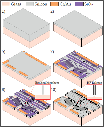
Our engineers reviewed the schematics and suggest two options for the client to consider:
(1) Option 1 - Using SOG wafer per discussion. The polymer bonding agent is to work fine with client's
process flow. Buffered HF for his application won't damage the bonding at the chip banks. After DRIE, and before carrying on HF release, the client needs to use O2 plasma to remove expose polymer, it will be very clean and
polymer beneath comb fingers will be removed as well by allowing O2 plasma to purge wafer longer.
However, there is a second choice of manufacturing technology for this as Option 2 we propose
below.
(2) Option 2 – No need to use a specialty SOG wafer, this MEMS comb drive structure can be realized by using a double Si wafer bonded together with pre-defined
cavities.
Step 1. Starting with a standard silicon wafer with tox on both sides (note, tox serves as isolation to two electrodes), tox layer is patterned and using this layer as a shadow mask, a Si DRIE or RIE
process is carried on to form cavities with a certain depth, for example 10um to several tens microns. As our plant commercially produce thin Silicon wafers (see UW's website for capabilities), we can directly bond an
available 40um or 50um thick thin Si wafer onto the Si cavity wafer. The top thin Si wafer is originally prepared with PECVD oxide on top side, it can be predefined with Cr/Au for electrodes as well. Then, using the client's
mask for Si DRIE to form etch-through trench. At last, O2 plasma etch to remove expose polymer to float the entire structure.
We believe Option 2 is better because (a) our plant has a very matured technology
that enables perfect bonding of a thin Silicon wafer with a cavity Si wafer by using a specialty polymer as bonding agent, as thin as 1um; (b) it eliminates long-time HF release which may damage metal electrodes and may have
other uncertainties such as undercut depth uniformity and stiction; (c) no need to involve a customer-made SOG wafer; (d) you don't need to use Cr/Au here either as isolated Si section itself function as electrode, of course if
client prefer wire bonding for electrical testing, Cr/Au can be incorporated into the process.
For Option 2: (A) our plant can act as foundry by provide manufacturing wafers, we can also dice and sort dies for shipment.
(B) Or if client wants to carry on process on his own, then our plant can provide bonded cavity wafer with alignment mark on wafer top so that client can easily work to complete the rest of the process steps including DRIE,
Dicing, etc.
If interested, please let us know, we can discuss more details.
142634
We use a spin-on specialty polymer material for bonding, bonding temperature <200C, and after which the bonded wafer can survive 200C. We can bond Si to most glass materials including fused silica as long as both surfaces are
clean and polished. Let me know if interested.
142690
The plant will use the wafers provided by the client to manufacture SOG wafers with specified thickness and TTV. (Will you supply the wafers or do you want us to source them?)
The polymer bonding material is able to withstand KOH and HF environments and compatible with general cleanroom agents such as Acetone, Methanol, etc., can withstand temperature up to 200C, can be patterned by using O2 plasma to
etch. To mate together the silicon and glass after, the polymer thickness an be controlled to 2+/-1um thickness and free of void and pin holes, that is 100% surface engagement.
Quote below:
Client provide wafer materials for the plant to work on.The plant provide wafer bonding service and which grind/lapping/polishing Si side to 50+/-5um thickness.
Minimum order: 5 wafer pairs to produce 5 pieces of 4" SOG wafers. Price/wafer: $378.90. Lead time: 3-5 weeks.
For order qyt of 10-25 wafer pairs, that produces 10-25 SOG wafers, price/wafer: $292.90, lead time: 3-5 weeks.
For order qty of 25-50 wafer pairs, that produces 25-50 SOG wafers, price/wafer: $275.90, lead time: 3-5 weeks.
For order qty of 50-100 wafer pairs, that produces 50-100 SOG wafers, price/wafer: $258.00, lead time: 3-5 weeks.
For order qty of 100 wafer pairs or more, that produces >100 SOG wafers, price/wafer: $223.90, lead time: 3-5 weeks.
For volume production >500 wafers, price/wafer drops to $189.90, lead time: 3-5 weeks.
If the plant just provide bonding service, not to reduce Si thickness afterwards, the price/wafer above is $85 LESS per wafer. In this case, the client can easily find a wafer grind/lapping/polish company to handle the job.
143051
could you send me more information about the buried polymer layer instead of thermal oxide an I am also interested in your PMN-PT material.
The polymer layer is spin on before bonding, the material is resistant to KOH etching and resistant to HF etchant as well. It can withstand 158C long term and can be etched by O2 plasma quickly.
The benefits lies for MEMS community in that wafers with polymer buried layer instead of thermal oxide has much less stress, and as a result, in releasing MEMS structure, the thin (for
example 2um-20um thick) MEMS features won't  be deformed due to tox. The deformed MEMS features will cause problem in RIE silicon etching and cause structure stiction to supporting
substrate. Also, the polymer buried layer can be easily clean by dry method such as O2 plasma.
|

